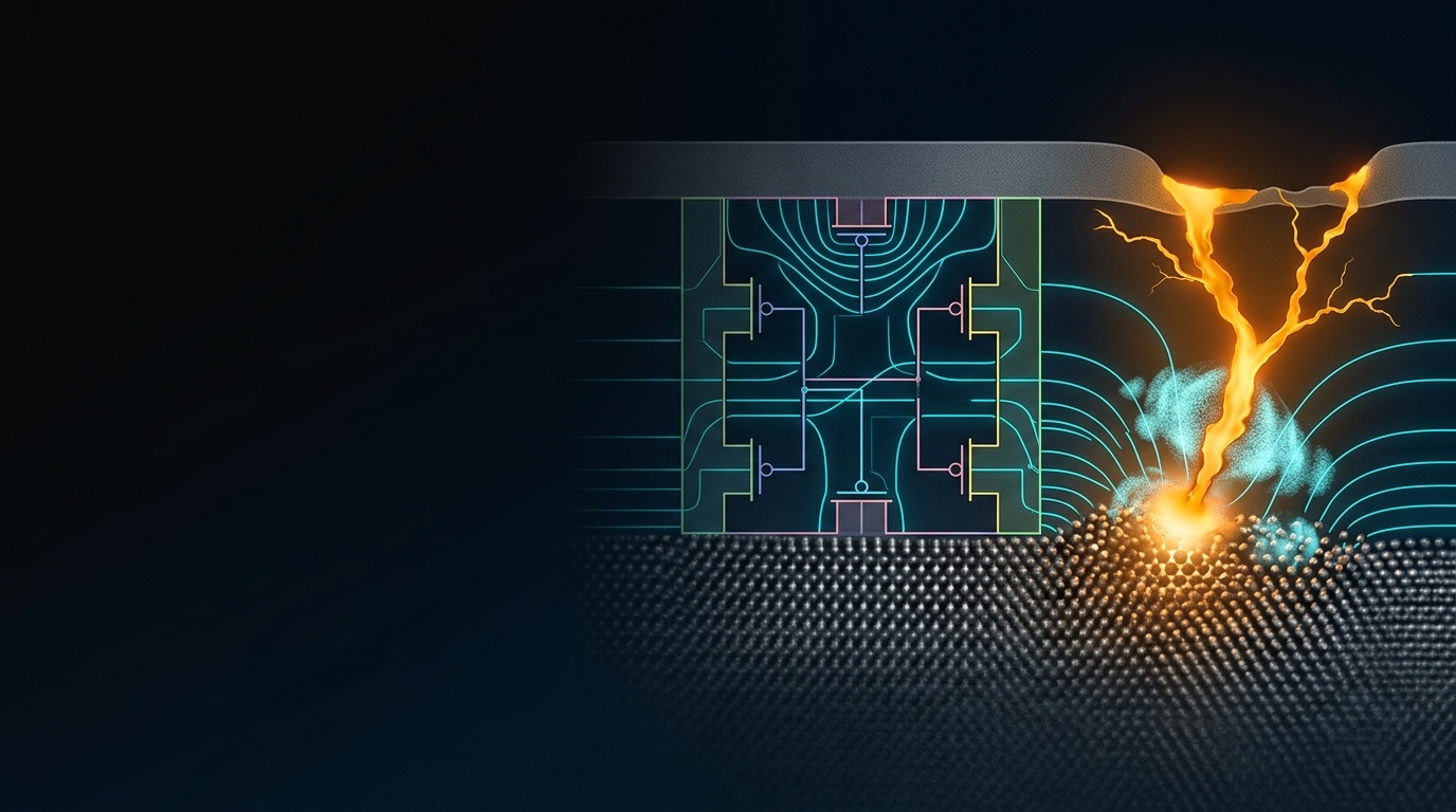
Memory Physics & Hardware Security Bitcell Microarchitecture Visual

研究筆記 02 · 記憶體物理與硬體安全RESEARCH NOTE 02 · MEMORY PHYSICS & HARDWARE SECURITY

可量產的互補式儲存,
形成可驗證的差異
Scalable complementary storage
creates a verifiable difference

第一性原理:實體安全不是數學孤島,而是由微觀位元胞物理決定的經濟學與可觀察度賽局。 First Principles: Hardware security is not a mathematical silo, but an economic & observability contest dictated by bitcell physics.

感測器可以比較 voltage 或 current;產品真正拉開差距的,是 bit-cell economics 能否支撐 complementary representation、降低一階資料相依訊號,再由 SRAM PUF、加密 OTP 與 secure controller 封閉完整攻擊鏈。 A sense amplifier may compare voltage or current. Product differentiation comes from bit-cell economics that make complementary representation practical, suppress first-order data-dependent signatures, and combine with SRAM PUF, encrypted OTP and a secure controller to close the attack chain.

27核心來源CORE SOURCES
5分析層級ANALYSIS LAYERS
SRAM ↔ OTP主要比較軸PRIMARY AXIS
2026-08-12研究版本RESEARCH VERSION
法則 #01RULE #01
ΔV / ΔI 差動感測ΔV / ΔI DIFFERENTIAL
差動感測 · 抵消共模雜訊Common-Mode Noise Rejection
互補表示可降低一階資料相依訊號;平衡程度仍需量測Complementary representation can reduce first-order signatures; balance requires measurement
03 · 架構與成本邊界03 · Architecture and cost limits
法則 #02RULE #02
物理觀測極限OBSERVABILITY LIMITS
可觀察性須依實作與設備驗證Observability Depends on Implementation
Antifuse 已有 FIB-PVC 擷取實證,不能一概視為不可讀Antifuse extraction by FIB-PVC is demonstrated; unreadability is not universal
05 · 實證與供應商測試05 · Demonstrations and vendor tests
法則 #03RULE #03
SRAM PUF 金鑰重建SRAM PUF KEYGEN
按需重建未永久儲存的根金鑰Reconstruct a Non-Stored Root on Demand
仍須驗證關機條件、資料殘留與上電重建保護Shutdown, remanence and powered reconstruction still require validation
04 · 互動讀取與條件04 · Interactive read and conditions
法則 #04RULE #04
縱深防禦體系LAYERED PROTECTION
階層化安全邊界隔離Attack Surface Separation
PUF 根與 OTP 密文透過專屬硬體控制器解耦Hardware controller decouples key roots from memory
08 · 系統後果與前提08 · System consequences and assumptions

摘要 · 核心發現ABSTRACT · CENTRAL FINDING

學術上可行,不等於產品上值得Circuit feasibility is not product feasibility

典型高速 6T SRAM 以 BL/BLB 的小擺幅 ΔV 讀取;current-mode SRAM 在文獻與專利中存在,但不是主流 compiled SRAM 的商業選擇。Antifuse OTP 也可做 differential sensing,然而安全價值取決於「資料本身是否由互補 cell pair 表示」,而不只是 sense amplifier 比較兩個端點。這正是 bit-cell 面積、routing、programming 與良率成本開始主導產品決策的位置。Mainstream high-speed 6T SRAM reads a small ΔV across BL/BLB. Current-mode SRAM exists in papers and patents, but it is not the mainstream commercial choice for compiled SRAM. Antifuse OTP can also use differential sensing; however, the security value depends on whether the data itself is represented by a complementary cell pair—not merely whether a sense amplifier compares two inputs. This is where bit-cell area, routing, programming and yield economics dominate the product decision.

安全上的根本分界是 state persistence。未供電 SRAM 不維持邏輯 0/1,但製程 mismatch 仍是可在下次上電表達的物理來源;已 programming/enrollment 的 OTP、eFuse、antifuse 或 NeoPUF 則保留可重複表達的永久物理狀態。這使攻擊時間窗、可用失效分析工具、zeroization 能力與擷取後果本質不同。The security divide is state persistence. Unpowered SRAM no longer maintains logical 0/1, although process mismatch remains to be expressed at the next power-up. Programmed or enrolled OTP, eFuse, antifuse and NeoPUF retain a persistent physical state. That changes the attack window, applicable failure-analysis tools, zeroization capability and consequence of extraction.

用語紀律:Terminology discipline: 本文不把 persistent PUF response 直接稱為「明文 key」。NeoPUF 公開資料描述的是 enrollment 後的永久 tunneling-path 位置,再由電流感測導出 PUF bit;是否直接等同某個最終 cryptographic key,取決於後續 key derivation 與產品實作。This paper does not equate a persistent PUF response with a plaintext key. NeoPUF literature describes a permanent enrolled tunneling-path location sensed into PUF bits; whether that equals a final cryptographic key depends on derivation and product implementation.

01 · 修正物理模型01 · CORRECT THE MODEL

先把三個直覺,
改寫成可驗證的命題
Turn three intuitions
into testable claims

安全比較必須區分 cell physics、read circuit、observable side channel 與 system consequence。把四層混成一句話,會同時低估 SRAM 攻擊與高估「current hotspot」的必然性。A security comparison must separate cell physics, read circuitry, observable side channels and system consequence. Collapsing the four layers understates SRAM attacks and overstates the inevitability of current hotspots.

01

SRAM 主流是 differential voltage readMainstream SRAM uses differential-voltage read

高速 6T SRAM 以 Q/QB、BL/BLB 的天然互補結構產生小擺幅 ΔV。current-mode 電路確實可行,但「可行」不代表它是量產 compiler 在速度、穩定度與功耗間的主流選擇。High-speed 6T SRAM naturally produces a small ΔV through complementary Q/QB and BL/BLB. Current-mode circuits are feasible, but feasibility does not make them the mainstream compiler choice across speed, stability and power.

電路與市場現實CIRCUIT + MARKET REALITY
02

OTP 並非「只能感測電流」OTP is not current-only

cell 的高/低導通確實常是資訊來源,但 sensing 可以比較 current、voltage、charge 或 time。antifuse OTP 專利明確揭露 differential-voltage bitline sensing。High or low cell conduction is often the information source, but sensing can compare current, voltage, charge or time. Antifuse OTP patents explicitly disclose differential-voltage bitline sensing.

專利證據PATENT EVIDENCE
03

「亮點」不是 current-sense 的同義詞A hotspot is not synonymous with current sensing

可偵測光/熱取決於局部電場、載子能量、漏電、電流密度、積分時間、背面光學路徑與噪音。已證明閒置 SRAM 也可因 state-dependent leakage 產生可辨識光子訊號。Detectable light or heat depends on local field, carrier energy, leakage, current density, integration time, backside optics and noise. Idle SRAM has been read through state-dependent leakage photons.

攻擊實證ATTACK EVIDENCE

02 · 第一性原理物理02 · FIRST-PRINCIPLES PHYSICS

量子穿隧、微絲滲透崩潰
與次閾值熱力學極限
Quantum Tunneling, Filament Percolation
and Subthreshold Thermal Limits

記憶體儲存機制與物理安全性,根植於微觀半導體物理。以下推導三組決定穿隧臨界、介電質永久破壞與靜態待機漏電的第一性原理方程式,作為跨製程選型與側信道分析的物理基底。 Memory storage mechanisms and physical security are rooted in device physics. Below are three sets of first-principles equations governing tunneling thresholds, permanent breakdown and subthreshold leakage.

量子傳輸QUANTUM TRANSPORT

Fowler–Nordheim (FN) 穿隧與能障幾何 Fowler–Nordheim Tunneling & Barrier Physics

JFN = AFN Eox2 exp(−BFN / Eox)
  • 三角形能障 (FN 穿隧):當跨氧化層電壓 Vox > ΦB/q 時發生。理論係數 BFN = [4√(2m*)(qΦB)3/2] / (3qℏ)。在 Si-SiO2 界面 (ΦB ≈ 3.15 eV, m* ≈ 0.5m0) 下,理論值約 2.70 × 10⁸ V/cm (270 MV/cm);計入影像力降低與介面態經驗值常修訂為 2.48 ∼ 2.50 × 10⁸ V/cm。 Triangular Barrier (FN Tunneling): Occurs when Vox > ΦB/q. Theoretical coefficient BFN = [4√(2m*)(qΦB)3/2] / (3qℏ) ≈ 2.70 × 10⁸ V/cm for Si-SiO2B ≈ 3.15 eV, m* ≈ 0.5m0), with experimental values around 2.48–2.50 × 10⁸ V/cm.
  • 梯形能障 (Direct Tunneling):tox ≤ 3.0 nm 且 Vox < ΦB/q 時,載子直接穿越完整梯形位障,穿隧電流對厚度呈現極端指數相依性 JDT ∝ exp(−α · tox)。此為厚度極限微縮下的主要漏電來源。 Trapezoidal Barrier (Direct Tunneling): When tox ≤ 3.0 nm and Vox < ΦB/q, carriers traverse a trapezoidal barrier with exponential thickness sensitivity JDT ∝ exp(−α · tox).
介電質崩潰DIELECTRIC BREAKDOWN

介電質 4 階段滲透崩潰微觀物理 4-Stage Dielectric Percolation Breakdown

AntiFuse OTP 的不可逆導通多遵循閘極氧化層滲透崩潰(Percolation Model)四階段。NeoPUF 公開資料描述受控軟崩潰與量子穿隧路徑的限流/負回授,以避免硬崩潰;不得把下方熔融矽微絲模型直接套用到 NeoPUF enrollment。 AntiFuse OTP irreversible conduction often follows four percolation-breakdown stages. NeoPUF vendor literature describes controlled soft breakdown with tunneling-path current limiting — not the hard-collapse silicon-filament model below.

01 · 陷阱累積01 · TRAP ACCUMULATION

高電場 (>10 MV/cm) 注入電子激發陽極電洞,中性氧空缺 (VO) 缺陷隨時間隨機累積。High-field electron injection triggers anode hole generation; neutral oxygen vacancies (VO) accumulate stochastically.

02 · 軟崩潰 (SBD)02 · SOFT BREAKDOWN (SBD)

缺陷密度達到滲透臨界 Nbd ≈ 1019∼1020 cm−3,形成非彈性聲子輔助穿隧點狀路徑,顯著表現 RTN 噪聲。Defect density reaches threshold Nbd ≈ 1019–1020 cm−3, initiating localized phonon-assisted tunneling with RTN noise.

03 · 硬崩潰 (HBD)03 · HARD BREAKDOWN (HBD)

局部電流密度急遽攀升,焦耳熱功率失控引發熱失控,溫度瞬間突破矽熔點 (>1414°C)。Current density spikes, causing thermal runaway with local temperatures exceeding the Si melting point (>1414°C).

04 · 矽微絲成型(AntiFuse 教學模型)04 · SILICON FILAMENT (ANTIFUSE MODEL)

部分硬崩潰 AntiFuse 文獻描述局域再結晶導通路徑;形貌與電阻取決於堆疊、應力與程式化條件,非固定 3–8 nm/<100 Ω 常數。NeoPUF 以穿隧電流讀出,不應套用此熔融微絲敘述。Some hard-breakdown AntiFuse literature describes a localized recrystallized conduction path; morphology and resistance depend on stack, stress, and programming — not fixed 3–8 nm / <100 Ω constants. NeoPUF readout uses tunneling current and must not inherit this melt-filament narrative.

擴散與漏電DIFFUSION & LEAKAGE

次閾值擴散漏電與 60 mV/dec 熱力學極限 Subthreshold Diffusion & 60 mV/dec Limit

Isub = μ Cox (W/L) (kBT/q)2 (m−1) exp[(VgsVth)/(m kBT/q)] [1 − exp(−qVds / kBT)]
  • 弱反轉擴散電流:載子濃度受玻爾茲曼分佈支配,次閾值擺幅 S = ln(10) · (kBT/q) · m,其中體效應因數 m = 1 + Cdep/Cox > 1。在室溫 300 K 下熱電壓 kBT/q ≈ 25.85 mV,理論極限為 59.5 mV/dec ≈ 60 mV/dec Weak Inversion Diffusion: Governed by Boltzmann statistics; subthreshold swing S = ln(10) · (kBT/q) · m where m = 1 + Cdep/Cox > 1. At 300 K (thermal voltage ≈ 25.85 mV), the physical thermodynamic limit is 59.5 mV/dec ≈ 60 mV/dec.
  • SRAM 待機功耗本質:6T SRAM 關閉通道仍受次閾值漏電與閘極穿隧制約,隨結溫升高呈指數級惡化;而 AntiFuse 的已編程微絲為永久金屬態/歐姆通道,未編程單元待機漏電 <0.01 pA/cell,具備極致低功耗靜態優勢。 Standby Power Implications: 6T SRAM remains bounded by subthreshold diffusion and gate tunneling, degrading exponentially at elevated junction temperatures. In contrast, unprogrammed AntiFuse cells exhibit sub-0.01 pA/cell leakage.

03 · 商用量產現實03 · COMMERCIAL REALITY

差動讀取不難畫;
量產成本決定商業可行性
Differential read is easy to draw;
production cost determines viability

真正該比較的不是 sense amplifier 的名稱,而是每個 logical bit 要付出多少 cell、金屬線、programming 操作與 array overhead,才能形成真正的 complementary representation。The meaningful comparison is not the sense-amplifier label, but how many cells, wires, programming operations and array overheads each logical bit must pay to create a genuinely complementary representation.

決策重點EXECUTIVE TAKEAWAY Differential sensing 是電路能力;complementary storage 的成本,是重要的 IP 差異化條件。Differential sensing is a circuit capability; complementary-storage cost is a material IP differentiator.

一個 data cell 與固定 reference 比較,仍是 single-ended physical representation。只有「同一 logical bit 以一對互補 cell 表示」時,0/1 的總體活動才有機會在一階近似下趨於對稱。Comparing one data cell against a fixed reference remains a single-ended physical representation. Only when one logical bit is stored as a complementary cell pair can aggregate 0/1 activity approach first-order symmetry.

01結構性天然互補COMPLEMENTARY BY CONSTRUCTION
揮發性 (6T)VOLATILE (6T)

6T SRAM

6T/一個互補 logical bit/ one complementary logical bit

儲存節點 Q/QB 與讀取線 BL/BLB 天然成對;高速主流實作以 small-swing differential voltage sensing 放大兩線差值。Storage nodes Q/QB and read lines BL/BLB are paired by construction; mainstream high-speed implementations amplify a small differential-voltage swing.

02經濟考量之單端讀取SINGLE-ENDED BY ECONOMICS
單端 (~4D)SINGLE-ENDED (~4D)

傳統 2-device AntifuseConventional 2-device Antifuse

2D + 2D ≈ 4D/互補 logical bit 的 device-count 抽象/ device-count abstraction for a complementary bit

常見 cell 由 select device 加 antifuse device 組成;若把 single-ended data+reference 升級為真正 complementary pair,需再付一組 cell、routing 與 programming 成本,因此商用品多選 single-ended 讀取。A common cell combines a select device and an antifuse device. Upgrading single-ended data-plus-reference to a true complementary pair adds another cell, routing and programming burden, so commercial products often remain single-ended.

03實用密度下的差動架構DIFFERENTIAL AT PRACTICAL DENSITY
差動 (2T)DIFFERENTIAL (2T)

Synopsys 1T OTP 差動單元Synopsys 1T OTP

1T + 1T ≈ 2T/互補 logical bit 的 device-count 抽象/ device-count abstraction for a complementary bit

Synopsys 的 patented split-channel 1T architecture 支援 twin-cell differential arrangement:一對 cell 中恰有一個被 programming。以 device count 觀察,互補 bit 的成本可接近傳統 2-device single-ended cell,讓 differential storage 成為可量產的商業選項。Synopsys' patented split-channel 1T architecture supports a twin-cell differential arrangement with exactly one programmed cell per pair. On a device-count basis, a complementary bit can approach the cost of a conventional single-ended two-device cell, making differential storage commercially practical.

面積紀律:Area discipline: 上圖只比較 bit-cell device count,不宣稱 macro area 等比例縮放。真實 PPA 還包含 charge pump、decoder、sense amplifier、ECC、redundancy、routing、test 與製程設計規則;應以同節點、同容量、同可靠度的 silicon report 封閉。The diagram compares bit-cell device count only; it does not claim proportional macro-area scaling. Real PPA also includes charge pumps, decoders, sense amplifiers, ECC, redundancy, routing, test and process design rules, and must be closed with same-node, same-capacity, same-reliability silicon data.

SYNOPSYS · 產品公開揭露SYNOPSYS · PRODUCT DISCLOSURE「可配置」differential read mode“Configurable” differential read mode

公開 technical article 直接把 differential mode 連結到降低 power-signature 辨識。The public technical article directly links differential mode to harder power-signature identification.

NeoPUF · 供應商公開揭露NeoPUF · VENDOR DISCLOSURE單端 Icell ↔ Iref 比較Single-ended Icell ↔ Iref

PUFsecurity 書籍以 cell current 與固定 reference 的比較描述 readout。PUFsecurity's book describes readout as cell current compared with a fixed reference.

TSMC · 晶圓廠發表論文TSMC · FOUNDRY PAPER5 nm 虛擬差動 (Pseudo-differential)Pseudo-differential at 5 nm

證明先進節點實作可行;論文不等同商業產品的 default security configuration。Proves advanced-node feasibility; a paper is not a commercial product's default security configuration.

本證據庫可防守的市場結論:Defensible market conclusion within this corpus: 在目前納入的公開商業資料中,Synopsys 是唯一明確把 configurable differential OTP read 作為安全能力對外說明的供應商。這是 corpus-bounded conclusion,不宣稱已證明全球所有未公開 macro 的唯一性。Among the public commercial materials reviewed here, Synopsys is the only vendor explicitly presenting configurable differential OTP read as a security capability. This is a corpus-bounded conclusion, not proof of exclusivity across every undisclosed macro worldwide.

架構表示REPRESENTATION

先問「資料怎麼存」Ask how data is stored first

Data cell 對 fixed reference 是 pseudo/reference differential;twin-cell 一正一反才是 complementary physical representation。A data cell against a fixed reference is pseudo/reference differential; a true-versus-complement twin cell is complementary physical representation.

一階平衡FIRST-ORDER BALANCE

0/1 的總活動趨於對稱Aggregate 0/1 activity approaches symmetry

若每次讀取都啟動一對互補 cell,總體導通與 bitline 活動較不直接暴露資料極性,可降低一階 power signature。Reading both complementary cells makes aggregate conduction and bitline activity less directly tied to data polarity, reducing first-order power signature.

非絕對力場NOT A FORCE FIELD

平衡不等於不可觀察Balance is not invisibility

空間解析的光學/FIB 攻擊仍可能分辨哪顆 cell 被 programming;layout balance、controller、ciphertext 與 ephemeral root 仍是必要防線。Spatially resolved optical or FIB attacks may still distinguish the programmed cell; balanced layout, controller policy, ciphertext and an ephemeral root remain necessary.

技術沿革與 TSMC 授權脈絡(研究註解)Technology provenance and TSMC licensing context (research note)

Research note (provenance — not product brand claim)研究註記(源流程,非產品品牌主張)

以 Synopsys 為主體:Synopsys is the product subject: 現行 Synopsys OTP portfolio 已整合多條技術血統。歷史上,split-channel 1T-Fuse 於 2017 年隨 Sidense 收購納入;Kilopass 的 1T/2T portfolio 則於 2018 年納入。這些原公司名稱只用於追溯專利與公開紀錄,不作為現行產品品牌。The current Synopsys OTP portfolio integrates multiple technology lineages. Historically, split-channel 1T-Fuse entered through the 2017 Sidense acquisition, while the Kilopass 1T/2T portfolio entered in 2018. Former company names are used only to trace patents and public records, not as current product brands.

TSMC 產業脈絡:TSMC industry context: 產品團隊的實務脈絡是:TSMC 10 nm 以下 in-house OTP 技術來自向 Synopsys(原 Kilopass 技術血統)取得授權。公開資料可旁證 TSMC/Kilopass 的早期 qualification、Synopsys 後續收購與 TSMC 5 nm antifuse 實作,但未公開授權合約本身。適合留在網站研究註解,不作為 TSMC OIP 台上主線。The product team's industry context is that TSMC's sub-10 nm in-house OTP technology was licensed from Synopsys (original Kilopass lineage). Public records corroborate early TSMC/Kilopass qualification, the later Synopsys acquisition and TSMC's 5 nm antifuse implementation, but not the license contract itself. This belongs in a website research note, not the main TSMC OIP stage narrative.

04 · 互動式讀取路徑04 · INTERACTIVE READ PATH

從 power-off 到 sense output,
逐層看差異在哪裡
From power-off to sense output,
locate the real divide

架構級四種讀取模式(單端/冗餘/差動/差動+冗餘)示意與取捨:technology-comparison · 讀取模式Architecture-class four read modes (single-ended / redundant / differential / differential+redundant): technology-comparison · Read Modes.

切換三個階段。左側代表 SRAM/SRAM PUF 的 volatile state expression;右側代表 programmed antifuse/NeoPUF 類 persistent conduction state。圖為 threat-model abstraction,不是特定 foundry macro schematic。Switch among three phases. The left abstracts volatile SRAM/SRAM-PUF state expression; the right abstracts a programmed antifuse/NeoPUF persistent conduction state. This is a threat-model abstraction, not a foundry-macro schematic.

SRAM / SRAM PUF揮發性閂鎖VOLATILE LATCH
感測 ΔV / ΔISENSE ΔV / ΔI
目前可觀察量CURRENT OBSERVABLE無邏輯狀態No logical state
反熔絲ANTIFUSE / NeoPUF持久路徑PERSISTENT PATH
ICELL ↔ IREF 比較ICELL ↔ IREF
目前可觀察量CURRENT OBSERVABLE永久導通路徑Permanent conduction path
01

斷電:差異先出現在「狀態是否仍可被表達」Power-down: The divergence first appears in whether state can still be represented

SRAM latch 沒有供電,不再維持 0/1 邏輯狀態;但製程 mismatch 仍存在。已 enrollment 的 antifuse/NeoPUF 導通路徑則是永久實體狀態。Unpowered SRAM latches no longer maintain a 0/1 logic state, although physical mismatch remains. Enrolled AntiFuse / NeoPUF conduction paths constitute permanent physical states.

關鍵細節:Key nuance: 在已驗證的 shutdown 條件下,設計不保留刻意儲存或仍由電源維持的 reconstructed root;這不代表晶片上沒有可量測的製程差異、helper material 或 remanence 風險。安全性仍依賴 response 不被輕易建模/成像、reconstruction 流程受保護、helper data 有 integrity,以及工作金鑰的 residency 與 zeroization 被控制。Under a validated shutdown condition, the design retains no intentionally stored or powered reconstructed root; this does not mean measurable process variation, helper material or remanence risk disappears. Security still depends on resisting characterization, protecting reconstruction, authenticating helper data, and controlling working-key residency and zeroization.

05 · 熱、光與可觀察性05 · HEAT, LIGHT & OBSERVABILITY

讀 0、讀 1 會不會形成
物理熱點或亮點
Does reading 0 or 1 create
a thermal or optical hotspot

答案是「可能形成 data-dependent contrast,但不是由 current-sense 這個名稱保證」。任何讀取都有能量;能不能被看見,取決於能量在空間與時間上是否集中到超過儀器、封裝與背景噪音的門檻。The answer is “data-dependent contrast may exist, but the label current-sense does not guarantee it.” Every read consumes energy; visibility depends on whether that energy is spatially and temporally concentrated above instrumentation, packaging and noise limits.

分析邊界 · 原始 OTP 元件ANALYSIS BOUNDARY · RAW OTP PRIMITIVE這一節只回答「OTP cell 能不能被看見」,還沒有回答「secret 能不能被還原」。This section asks whether OTP cells can be observed—not whether the secret can be recovered.

若 raw OTP 直接保存 plaintext,物理 readout 就可能完成資料揭露;若 OTP 保存的是由 PUF root 保護的 encrypted、address-scrambled data,cell-level reverse engineering 只完成攻擊鏈的第一段。If raw OTP directly stores plaintext, physical readout may complete disclosure. If OTP stores encrypted, address-scrambled data protected by a PUF root, cell-level reverse engineering completes only the first segment of the attack chain.

SRAM

動態讀取會產生 bitline charging/discharging 與 sense-amplifier switching;靜態保存也有 state-dependent leakage。Dynamic reads charge/discharge bitlines and switch the sense amplifier; static retention also has state-dependent leakage.

  • 已證明:Photon Emission、TLS、EOFM 可讀出 SRAM 內容。Demonstrated: Photon Emission, TLS and EOFM can recover SRAM contents.
  • 亮點位置可隨儲存 0/1 對應到不同 NMOS leakage path。Emission location can change with the NMOS leakage path selected by stored 0/1.
  • 需要供電、殘留狀態,或特定熱刺激/量測配置。Requires power, remanent state, or a specific thermal-stimulation setup.
Plocal = V · I必要能量 ≠ 保證可觀測NECESSARY ENERGY ≠ GUARANTEED OBSERVABILITY

OTP / OTP-PUF

programmed path 的 Icell 與 unprogrammed leakage 不同;局部 Joule heating 與 emission 在物理上可能,但量測可見度必須實驗驗證。A programmed path's Icell differs from unprogrammed leakage. Local Joule heating and emission are physically possible, but observability must be experimentally validated.

  • NeoPUF 文件描述 Icell 與 Iref 的 single-ended 比較。NeoPUF literature describes a single-ended Icell-to-Iref comparison.
  • 同一份供應商資料報告其 InGaAs 測試未在 PUF array 找到可區分 hotspot。The same vendor publication reports no distinguishable PUF-array hotspot in its InGaAs test.
  • 獨立 FIB-PVC 已直接擷取 40 nm antifuse OTP,無須依賴正常 read emission。Independent FIB-PVC extracted 40 nm antifuse OTP without relying on normal-read emission.
直接實證 · SRAMDIRECT · SRAM

閒置 SRAM 也能「發光洩漏」Idle SRAM can leak through photons

HOST 2018 示範以 photon emission microscopy 讀取 idle FPGA block RAM;光子來自 SRAM cell 中 state-dependent NMOS leakage。HOST 2018 demonstrated idle FPGA block-RAM readout using photon emission microscopy from state-dependent NMOS leakage.

DOI 10.1109/HST.2018.8383889 ↗
供應商 · NeoPUFVENDOR · NeoPUF

永久 path 不等於必然可見 hotspotA persistent path does not guarantee a visible hotspot

PUFsecurity 書籍描述 tunneling current readout,也報告其特定 InGaAs 實驗中 PUF array 未出現可分辨 hotspot。這是供應商證據,需獨立重現才可升級。PUFsecurity describes tunneling-current readout and reports no distinguishable PUF-array hotspot in its InGaAs experiment. This is vendor evidence pending independent replication.

Quantum Tunneling PUF, pp. 50–67 ↗
車規 · AEC-Q100 溫度分級AUTOMOTIVE · AEC-Q100 TEMPERATURE GRADES

溫度分級與資料保持能力須分別驗證Validate Temperature Grade and Data Retention Separately

AEC-Q100 Rev. J 將 Grade 0 定義為 −40°C 至 +150°C 的環境操作溫度範圍;175°C 結溫或應力條件不能直接當成 Grade 0 的分級定義。不同記憶體的儲存變數與失效機制不同,仍須依目標製程、程式寫入分布、讀取裕度、老化與工作條件驗證。更高結溫、15 年保持能力或零漂移均需相應產品測試,本頁不作無條件保證。AEC-Q100 Rev. J defines Grade 0 as an ambient operating range of −40°C to +150°C; a 175°C junction or stress condition is not the grade definition. Memory classes have different storage variables and failure mechanisms, requiring validation of the target process, programming distribution, read margin, aging and operating conditions. Higher junction temperatures, 15-year retention and zero drift each require product-specific test evidence; this page makes no unconditional guarantee.

AEC-Q100 Rev. J · §1.3.4, Table 1 ↗
特種高壓 · 核心氧化層與 BCD CASCODESPECIALTY HV · CORE OXIDE & BCD CASCODE

高壓製程須分開檢查寫入、隔離與待機漏電Check Programming, Isolation and Standby Leakage in High-Voltage Processes

BCD 與電子紙驅動的高壓條件(40V–50V),不能直接視為 OTP 位元胞本身的耐受電壓。Antifuse 係以原生低壓核心薄氧化層作為擊穿單元,形成永久閘極介電質擊穿微絲 (Permanent Gate-Dielectric Breakdown Filament / Localized Silicon Percolation Path),並依賴外圍高壓開關與 Cascode 隔離架構阻絕高壓衝擊。零光罩相容性、高壓隔離耐受、sub-pA 待機漏電與長期穩定度須分別附上目標 macro 的規格與測試條件;本頁未提供足以支持全面免疫的產品級證據。High-voltage conditions in BCD and electronic-paper drivers (40V–50V) do not directly define the OTP bitcell's intrinsic dielectric rating. Antifuse utilizes native low-voltage core thin oxide as the breakdown element to form a permanent gate-dielectric breakdown filament (localized silicon percolation path), relying on peripheral high-voltage switches and cascode isolation architectures to block high-voltage stress. Zero-mask compatibility, HV isolation tolerance, sub-pA standby leakage and long-term stability each require target-macro specifications and test conditions. This page does not provide product-level evidence for universal immunity.

09 · 檢視產品級驗證缺口09 · Review product-level evidence gaps
直接實證 · 反熔絲DIRECT · ANTIFUSE

攻擊者不需要等 memory 自己亮The attacker need not wait for the memory to emit

WOOT 2025 以 FIB passive voltage contrast 從 40 nm gate-dielectric-breakdown antifuse 擷取資料,證明失效分析 contrast 本身就是攻擊面。WOOT 2025 extracted data from 40 nm gate-dielectric-breakdown antifuses using FIB passive voltage contrast, making failure-analysis contrast itself the attack surface.

USENIX WOOT 2025 ↗

06 · 記憶體物理分類學06 · MEMORY TAXONOMY

「非揮發性」不是一種物理;
每一類留下不同痕跡
Nonvolatile is not one physics;
each class leaves a different trace

安全審查應先問 storage variable 是 latch state、charge、resistance、filament、phase、magnetization 還是永久結構,再選擇 imaging、stimulation、fault 與 side-channel 假設。A security review should first identify whether the storage variable is latch state, charge, resistance, filament, phase, magnetization or permanent structure, then select imaging, stimulation, fault and side-channel assumptions.

依儲存變數比較記憶體;技術分類不等同安全資格Memories by storage variable; a technology class is not a security qualification
技術Technology儲存/表達的變數Stored / expressed variable典型讀取觀測量Typical read observable斷電狀態Power-off state與安全相關的物理途徑Security-relevant physical avenues
SRAM / SRAM PUFSRAM / SRAM PUF
揮發性回應VOLATILE RESPONSE
cross-coupled latch 的 0/1;PUF 使用 power-up preference,其來源是 transistor mismatch。Cross-coupled-latch 0/1; PUF uses power-up preference rooted in transistor mismatch.位元線 ΔV、ΔI 與時序;啟動回應。Bitline ΔV, ΔI, timing; startup response.沒有 powered logic state;mismatch 仍在,下次上電表達。No powered logical state; mismatch remains and is expressed at next power-up.PEM、TLS、LLSI/EOFM、雷射故障、低溫殘留與輔助資料操控。PEM, TLS, LLSI/EOFM, laser fault, low-temperature remanence, helper-data manipulation.
電子熔絲 (eFuse)eFuse
持久結構PERSISTENT STRUCTURE
金屬 link 的完整/熔斷或電阻改變。Intact/blown metal link or resistance change.電阻/電流/衍生電壓。Resistance / current / derived voltage.永久幾何與電阻差異。Persistent geometric and resistive difference.光學/SEM 成像、PVC、探測、局部修復/編修與位址重建。Optical/SEM imaging, PVC, probing, focused repair/edit, address reconstruction.
反熔絲 (Antifuse) / NeoPUFAntifuse / NeoPUF
持久路徑PERSISTENT PATH
programmed conductive path;NeoPUF 為成對 MOS oxide 中 enrollment 後的 tunneling-path 位置。Programmed conductive path; NeoPUF uses the enrolled tunneling-path location in paired MOS oxides.單元電流相對參考值、電阻,或位元線電壓/電荷。Cell current vs reference, resistance, or bitline voltage/charge.永久導通位置/路徑。Persistent conduction location/path.FIB-PVC、SEM/TEM 嘗試、可量測時的發光/熱對比,以及解碼器/讀取路徑故障。FIB-PVC, SEM/TEM attempts, emission/thermal contrast if measurable, decoder/read-path fault.
浮動閘極/電荷捕捉Floating-gate / Charge-trap
持久電荷PERSISTENT CHARGE
trapped charge 改變 transistor threshold voltage。Trapped charge shifts transistor threshold voltage.通道電流/Vth 電壓窗。Channel current / Vth window.電荷與閾值分布持續存在。Charge and threshold distribution persist.前處理後的 SEM/PVC、電荷對比、紫外線/雷射擾動、讀取閾值操控與殘留。SEM/PVC after preparation, charge contrast, UV/laser disturbance, read-threshold manipulation, remanence.
可變電阻 (ReRAM) / 相變化 (PCM)ReRAM / PCM
持久材料狀態PERSISTENT MATERIAL
conductive filament/ionic state 或 amorphous-crystalline phase。Conductive filament/ionic state or amorphous-crystalline phase.電阻/電流/切換時間。Resistance / current / switching time.材料狀態持續存在。Material state persists.電阻映射、熱敏感度、依堆疊而定的顯微觀測、受故障影響的選擇器與潛行路徑。Resistance mapping, thermal sensitivity, microscopy depending stack, faulted selectors and sneak paths.
磁阻記憶體 (MRAM)MRAM
持久磁性狀態PERSISTENT MAGNETIC
magnetic tunnel junction 的平行/反平行 magnetization。Parallel/antiparallel magnetization of a magnetic tunnel junction.穿隧磁阻。Tunnel magnetoresistance.磁化方向持續存在。Magnetization direction persists.磁場/熱故障、電阻讀出,以及受堆疊與尺度限制的磁性成像。Magnetic field/thermal fault, resistance readout, magnetic imaging subject to stack and scale.
特種高壓 eNVMSpecialty HV eNVM
製程/應用類PROCESS / APPLICATION CLASS
BCD/高壓 PMIC、閘驅、DDIC 等平台的嵌入式 NVM 需求;實作可為 0-mask OTP/MTP、eFlash、AntiFuse 或代工 Y-Flash 等具名路線,不得整類等同單一 antifuse 微絲或固定 0-mask 敘述。Embedded NVM on BCD/HV PMIC, gate-driver, and DDIC platforms; implementations include named 0-mask OTP/MTP, eFlash, AntiFuse, or foundry Y-Flash routes — do not collapse the class into one antifuse filament or universal 0-mask story.依巨集:單端/差動、電流或電阻窗;需對應具名 IP/PDK。Macro-dependent: single-ended/differential current or resistance window; cite named IP/PDK.持久狀態型態隨選型而異(電荷、導通路徑、浮閘等)。Persistent state depends on selected technology (charge, conduction path, floating gate, etc.).高壓脈衝、熱預算與隔離架構為系統/製程設計問題,非單一儲存物理保證。HV pulses, thermal budget, and isolation are system/process design concerns, not one storage-physics guarantee.

07 · 安全層級實質差異07 · SECURITY-LEVEL DIFFERENCES

揮發性降低靜態目標,
但把風險移到上電窗口
Volatility reduces the static target,
but moves risk into the powered window

下表不是「誰絕對安全」的排名,而是攻擊前提與後果的差異。Direct 代表已有公開實證;Conditional 代表依實作與攻擊配置;Reduced 代表經分層保護後後果下降,而非攻擊消失。This is not an absolute-security ranking. It compares attack prerequisites and consequences. Direct means publicly demonstrated; Conditional depends on implementation; Reduced means layered protection lowers impact rather than eliminating attack.

攻擊前提與擷取後果;非絕對安全排名Attack prerequisites and extraction consequences, without an absolute-security ranking
攻擊手法/物理屬性ATTACK / PROPERTYSRAM / SRAM PUFSRAM / SRAM PUF持久性 OTP / OTP-PUFPERSISTENT OTP / OTP-PUF安全儲存防護結果SECURE STORAGE CONSEQUENCE
斷電後靜態成像Unpowered static imaging條件相依CONDITIONAL
普通 0/1 latch state 消失;但 mismatch characterization、冷凍殘留與特定 TLS 技術仍須考量。Ordinary latch 0/1 disappears; mismatch characterization, cold remanence and specialized TLS still matter.
直接暴露DIRECT
永久結構/charge/path 可被材料或電性 failure-analysis contrast 觀察;antifuse FIB-PVC 已有實證。Persistent structure, charge or path can yield material/electrical failure-analysis contrast; antifuse FIB-PVC is demonstrated.
降低衝擊REDUCED IMPACT
若 OTP 只保存經驗證的 ciphertext,cell dump 不應直接等於 plaintext secret。If OTP contains authenticated ciphertext, a cell dump should not directly equal plaintext secret.
上電靜態光學讀出Powered optical state readout直接暴露DIRECT
PEM、TLS、EOFM/LLSI 已讀出 SRAM/BBRAM key。PEM, TLS, EOFM/LLSI have recovered SRAM/BBRAM keys.
條件相依CONDITIONAL
取決於 cell、current density、read cadence、optical access 與 countermeasure;不能由 current-sense 自動推定。Depends on cell, current density, read cadence, optical access and countermeasures; not implied by current sensing.
作用時間窗ACTIVE WINDOW
root reconstruction 與 working-key 使用仍需 side-channel、shield、sensor、timing 與 zeroization 防護。Root reconstruction and working-key use still require side-channel, shield, sensor, timing and zeroization defenses.
雷射故障注入Laser fault injection直接暴露DIRECT
可翻轉 SRAM cell、擾動 startup response、攻擊 crypto 與控制流程。Can flip SRAM cells, perturb startup response, and attack crypto/control logic.
條件相依CONDITIONAL
永久 cell 未必可逆,但 decoder、sense amp、permission、read timing 仍可被 fault。The persistent cell may not reverse, but decoder, sense amp, permission and read timing remain fault targets.
系統級檢查SYSTEM CHECKS
secure controller 必須檢查 fault、integrity、lifecycle 與 read authorization,而非只相信 bit-cell。The secure controller must verify fault, integrity, lifecycle and authorization rather than trusting the bit cell alone.
低溫資料殘留Low-temperature remanence直接暴露DIRECT
SRAM 與 SRAM PUF 都有公開研究;「斷電立即消失」必須限定在正常條件與已驗證窗口。Published for SRAM and SRAM PUF; “disappears immediately” must be bounded by validated normal conditions.
固有屬性INHERENT
非揮發 state 的目標本來就是長期 retention;低溫不是必要前提。Long retention is the design goal; low temperature is not a prerequisite.
密文保護CIPHERTEXT
persistent data 仍在,但其機密性轉由 encryption 與 root-key separation 承擔。Persistent data remains, but confidentiality moves to encryption and root-key separation.
銷毀/撤銷能力Zeroization / revocation快速但需驗證FAST BUT VERIFY
volatile working key 可清除/斷電,但 remanence、backup、register、cache 與 compiler behavior 都需驗證。Volatile working keys can be cleared or depowered, but remanence, copies, registers, caches and compiler behavior require validation.
不可逆寫入IRREVERSIBLE
OTP cell 無法擦除;只能透過 permission、zeroize mapping、crypto erasure 或 key revocation 使資料失效。OTP cells cannot be erased; invalidation relies on permission, zeroize mapping, crypto erasure or key revocation.
密碼學銷毀CRYPTO ERASURE
若資料以衍生 key 保護,撤銷 key hierarchy 可使永久 ciphertext 失去可用性。If data is protected by derived keys, revoking the hierarchy can render persistent ciphertext unusable.
量產與可靠性Production & reliabilityECC / 輔助數據ECC / HELPER
PVT、aging、startup noise 需要 characterization、helper data、ECC、health tests 與 integrity。PVT, aging and startup noise require characterization, helper data, ECC, health tests and integrity.
編程/感測裕度PROGRAM / SENSE MARGIN
需驗證 programming distribution、read margin、disturb、aging、radiation 與 reference drift。Programming distribution, read margin, disturb, aging, radiation and reference drift require validation.
架構責任鏈ACCOUNTABILITY
整合產品價值在跨 PUF、crypto、OTP、controller 的 qualification 與責任閉環。Integrated-product value lies in cross-PUF, crypto, OTP and controller qualification with clear accountability.

08 · 從駭客攻擊到產品防禦08 · FROM OTP HACKER TO PRODUCT RESPONSE

OTP 可以被 reverse;
不代表 secret 可以被 reverse
OTP may be reversed;
the secret should not be

RP2350 challenge 的關鍵教訓不是「所有 OTP 都不安全」,而是:當永久 memory 直接承載可用 secret,成功繞過 lock 或讀出 cell 就接近攻擊終點。Secure Storage 的設計目標,是改寫這個後果。The central RP2350 lesson is not that every OTP is insecure. It is that when permanent memory directly carries a usable secret, bypassing a lock or reading the cells approaches the end of the attack. Secure Storage is designed to change that consequence.

根本成因 → 架構回應ROOT CAUSE → ARCHITECTURE RESPONSE

把「能讀 OTP」與「能取得 secret」拆成兩個不同問題Separate “reading OTP” from “recovering the secret”

純 OTP 資料防護PURE OTP DATA PROTECTION

單元狀態 → 直接可用機密Cell state → usable secret

若 flag、key 或敏感資料以可直接使用的形式留在 OTP,voltage glitch、permission bypass、FIB 或其他 readout 一旦成功,memory reverse engineering 就可能直接成為資料揭露。If a flag, key or sensitive data remains in directly usable form in OTP, a successful voltage glitch, permission bypass, FIB or other readout can turn memory reverse engineering directly into disclosure.

RP2350 實戰教訓RP2350 LESSON
翻轉攻擊後果CHANGES THE CONSEQUENCE
SYNOPSYS 安全儲存架構SYNOPSYS SECURE STORAGE

單元狀態 → 混淆加密密文Cell state → scrambled ciphertext

SRAM PUF 在受控上電窗口重建不永久儲存的 root;AES-256 保護 OTP data;address scrambling 打亂 logical-to-physical mapping;Secure Controller 管理授權與資料路徑。即使 OTP array 被物理重建,也不能只靠 OTP reverse engineering 直接還原 plaintext。SRAM PUF reconstructs a root that is never permanently stored; AES-256 protects OTP data; address scrambling obscures logical-to-physical mapping; and the Secure Controller governs authorization and data paths. Even if the OTP array is physically reconstructed, OTP reverse engineering alone should not directly recover plaintext.

SRAM PUF 根金鑰SRAM PUF ROOTAES-256位址擾亂 (Scrambling)ADDRESS SCRAMBLING安全控制器SECURE CONTROLLER
安全儲存核心原則SECURE STORAGE PRINCIPLEOTP 逆向工程 ≠ 機密逆向工程OTP REVERSE ENGINEERING ≠ SECRET REVERSE ENGINEERING
01 · 實體接觸01 · PHYSICAL ACCESS

定位 memory array 與 read pathLocate the array and read path

decap、backside prep、FIB、SEM、optical 或 fault reconnaissance。Decap, backside preparation, FIB, SEM, optical or fault reconnaissance.

02 · 單元提取02 · CELL EXTRACTION

恢復 OTP bitstreamRecover the OTP bitstream

取得 address-scrambled 或部分合併的 cell state,仍可能需要 mapping 與 ECC reconstruction。Obtain address-scrambled or partially merged states that may still require mapping and ECC reconstruction.

03 · 密碼學屏障03 · CRYPTOGRAPHIC BARRIER

得到的是 ciphertextThe result is ciphertext

cell readout 不再直接等於 data disclosure;integrity protection 也應阻止可控修改被接受。Cell readout no longer directly equals data disclosure; integrity protection should also reject controlled modification.

04 · 短暫根金鑰04 · EPHEMERAL ROOT

另攻 reconstruction/use windowAttack reconstruction or use separately

必須在上電後攻擊 PUF processing、crypto、working key、controller 或授權輸出。The attacker must target PUF processing, crypto, working keys, controller or authorized output after power-up.

安全結論:Security conclusion: Address scrambling 增加 physical mapping 成本,但不能取代 encryption;AES-256 的價值也依賴 root lifecycle、mode、integrity 與 controller isolation。可防守的主張是「OTP physical analysis 不再直接等於 plaintext disclosure」,而不是「Secure Storage 無法被攻擊」。產品仍必須證明同一 fault、debug permission 或 controller flaw 不能把 root 與 ciphertext 路徑一次串通。Address scrambling raises physical-mapping cost but does not replace encryption; AES-256 also depends on root lifecycle, mode, integrity and controller isolation. The defensible claim is that OTP physical analysis no longer directly equals plaintext disclosure—not that Secure Storage cannot be attacked. The product must still show that one fault, debug permission or controller flaw cannot collapse the root and ciphertext paths together.

09 · 技術主張與證據邊界09 · TECHNICAL CLAIMS & EVIDENCE BOUNDARIES

物理抗噪裕度,
與一階功耗訊跡衰減
Physical Noise Margins
and First-Order Trace Attenuation

對半導體架構師與晶片設計團隊,可信度來自承認所有 silicon primitive 都有 attack surface,同時清楚說明整合架構如何降低成功攻擊的後果與組合機率。For silicon architects and chip designers, credibility comes from acknowledging that every silicon primitive has an attack surface while showing how integration reduces attack consequence and composition probability.

可以強力主張Defensible Claims

  • SRAM PUF root key 不以永久數位值儲存在 NVM;它在需要時重建。The SRAM-PUF root key is not stored as a permanent digital value in NVM; it is reconstructed when needed.
  • 1T AntiFuse OTP 的位元胞經濟性讓互補成對差動單元 (Complementary Twin-Cell) 在量產密度下具備實用可行性;能實質提供感測物理抗噪裕度與一階差分功耗 (DPA) 訊跡衰減。1T AntiFuse OTP bitcell economics make complementary twin-cell storage practical at volume density, providing measurable physical noise margin and first-order DPA side-channel attenuation.
  • SRAM PUF 降低斷電時可直接成像的 root-key logical state,但仍需防護 powered reconstruction。SRAM PUF reduces the directly imageable root-key logical state at power-off while still requiring protection during powered reconstruction.
  • AES-256 讓 OTP bit-cell extraction 不直接等於 plaintext disclosure,前提是 mode、integrity、nonce/tweak 與 key hierarchy 正確。AES-256 makes OTP bit-cell extraction differ from plaintext disclosure, provided mode, integrity, nonce/tweak and key hierarchy are sound.
  • PUF + crypto + OTP + controller 的預整合可降低跨 block 假設遺漏;qualification 範圍與契約責任仍需逐案確認。Pre-integrating PUF, crypto, OTP and controller can reduce missed cross-block assumptions; qualification scope and contractual accountability still require confirmation.
  • 供應商揭露的 SRAM PUF 量產紀錄可縮小成熟度不確定性,但不能取代當代節點與目標配置的 attack evaluation。Vendor-reported SRAM-PUF deployment history narrows maturity uncertainty, but does not replace attack evaluation on the current node and target configuration.
「永久保存資料,不永久保存 root key;即使 memory 被讀出,留下的仍是密碼學問題。」“Keep data permanent, not the root key; even after memory readout, a cryptographic problem remains.”

應避免的過度主張Claims to Avoid

  • 「SRAM 只感測電壓,所以沒有物理 emission。」“SRAM only senses voltage, therefore it has no physical emission.”
  • 「current-sense OTP 讀 0/1 一定會形成可見亮點。」“Current-sense OTP always creates visible 0/1 hotspots.”
  • 「斷電後 SRAM 的所有物理資訊都消失。」“All physical information in SRAM disappears at power-off.”
  • 「NeoPUF 就是把 plaintext key 寫進 OTP。」除非有產品級 key mapping 證據。“NeoPUF writes a plaintext key into OTP,” absent product-level key-mapping evidence.
  • 「只要加 AES 就安全。」若沒有 integrity、anti-replay、domain separation、fault control 與 secure lifecycle,仍可能失敗。“AES alone makes it secure.” Without integrity, anti-replay, domain separation, fault control and lifecycle security, the system can still fail.
誠實承認 active-window 攻擊面,不會削弱定位;它會把差異從 slogan 提升成 architecture。Acknowledging the active-window attack surface strengthens the message by elevating it from slogan to architecture.

10 · 證據紀律與邊界限制10 · EVIDENCE DISCIPLINE & LIMITS

每一個結論,
標示它站在哪一階
Every conclusion declares
which rung supports it

論文、專利與產品資料回答不同問題。專利證明可行的 circuit topology,不代表產品實作;供應商測試是重要證據,但獨立重現前不能與第三方攻擊示範同級。Papers, patents and product literature answer different questions. A patent establishes a possible topology, not product implementation. Vendor tests matter, but are not equivalent to independent attack demonstrations before replication.

E1 · 直接實體證據E1 · DIRECT

第三方實體示範Independent physical demonstration

實際晶片、攻擊設備、輸出與限制可追溯;例如 SRAM PEM/TLS 與 antifuse FIB-PVC。Traceable chip, equipment, output and limits; e.g. SRAM PEM/TLS and antifuse FIB-PVC.

E2 · 電路物理機制E2 · MECHANISM

電路/物理機制Circuit or physical mechanism

論文與專利支持 sensing、leakage、breakdown、reference 等機制,但不自動映射特定商用品。Papers and patents support sensing, leakage, breakdown and reference mechanisms without automatically mapping to a product.

E3 · 供應商公開揭露E3 · VENDOR

供應商公開揭露Vendor disclosure

可用於描述產品宣稱、architecture 與內部測試;必須清楚標記來源與獨立驗證狀態。Useful for product claims, architecture and internal tests; source and independent-validation status must be explicit.

E4 · 系統級推論E4 · INFERENCE

系統級推論System-level inference

由多項證據組合出的 threat-model 結論;需要產品規格、NDA data 或實驗才能封閉。A threat-model conclusion composed from multiple sources; closure requires product specs, NDA data or experiments.

仍需產品級回答Product-level questions still open

Secure Storage 的 AES mode 與 integrity、address scrambling 的 cryptographic role、PUF activation/helper-data integrity、root/working-key zeroization、debug/scan policy、fault sensor coverage、reset/brownout behavior、secure-region granularity,以及對 FIB/optical/EMFI 的實測證據。AES mode and integrity, the cryptographic role of address scrambling, activation/helper-data integrity, root/working-key zeroization, debug/scan policy, fault-sensor coverage, reset/brownout behavior, secure-region granularity, and measured resistance to FIB/optical/EMFI.

「所有 NVM」的限制Limits of the “all NVM” taxonomy

此頁將技術分成主要 storage variable,但實際安全取決於 process stack、cell topology、array layout、ECC、decoder、packaging、backside metal、sensor 與 operational protocol。不同 foundry node 不應直接外推。This page groups technologies by storage variable, but actual security depends on process stack, cell topology, layout, ECC, decoder, packaging, backside metal, sensors and protocol. Results should not be extrapolated across foundry nodes without validation.

結論 · 安全性是生命週期屬性CONCLUSION · SECURITY IS A LIFECYCLE PROPERTY

讓永久 state 可以被讀,
但不能直接變成永久 secret
Let persistent state be readable
without making it a persistent secret

更有保障的答案不是單一 bit-cell,而是可驗證的責任鏈:1T economics 讓 differential OTP 可量產;互補讀取降低一階資料相依訊號;OTP 保存耐久 ciphertext;具供應商量產紀錄的 SRAM PUF 在受控窗口重建未永久儲存的 root;crypto 與 controller 讓兩條攻擊路徑不直接合流。A stronger answer is not one bit cell but a verifiable chain: 1T economics make differential OTP practical; complementary read reduces first-order data-dependent signature; OTP retains durable ciphertext; a vendor-reported, production-deployed SRAM PUF reconstructs a root that is never permanently stored; crypto and controller keep the attack paths from collapsing into one.

檢視完整證據庫Inspect the evidence base 返回 Secure StorageReturn to Secure Storage