特種製程 NVM:類比微調、高壓顯示、矩陣修復與電子紙驅動 Specialty eNVM: Analog Trimming, HV Display, Matrix Repair & E-Ink Drivers
深入解析 BCD 電源管理(PMIC 微調、LED 驅動、USB-PD 快充協議、BLDC 馬達與 BMIC AFE)、高密集陣列缺陷修復(CIS 與 DRAM/HBM 冗餘重映射)、高壓 (HV) 顯示驅動(Gamma 2.2、Vcom、De-Mura),以及電子紙 (E-Ink) 40V-50V 超高壓電泳驅動與「演進期 MTP ➔ 成熟期 OTP」產品生命週期演進。配備 4 大旗艦級互動實驗室。 Deep treatise on BCD Power Management (PMIC trimming, LED drivers, USB-PD protocols, BLDC motor firmware, BMIC AFE), Dense Matrix Array Repair (CIS and DRAM/HBM redundancy remapping), High-Voltage Display Driver ICs, and E-Ink 40V-50V Ultra-HV driving with MTP-to-OTP lifecycle migration. Equipped with 4 flagship interactive laboratories.
特種半導體 4 大底層物理與邊界約束 Four Governing Microphysical Models & Foundry Boundaries
01 · BANDGAP 帶隙基準溫漂模型 01 · BANDGAP Reference Temp Drift Model
02 · POISSON 泊松介電擊穿統計 02 · POISSON Dielectric Breakdown Statistics
03 · GAMMA 2.2 亮度轉換 03 · GAMMA 2.2 Optical Transfer Function
04 · STOKES 斯托克斯電泳微粒流動 04 · STOKES Electrophoretic Particle Dynamics
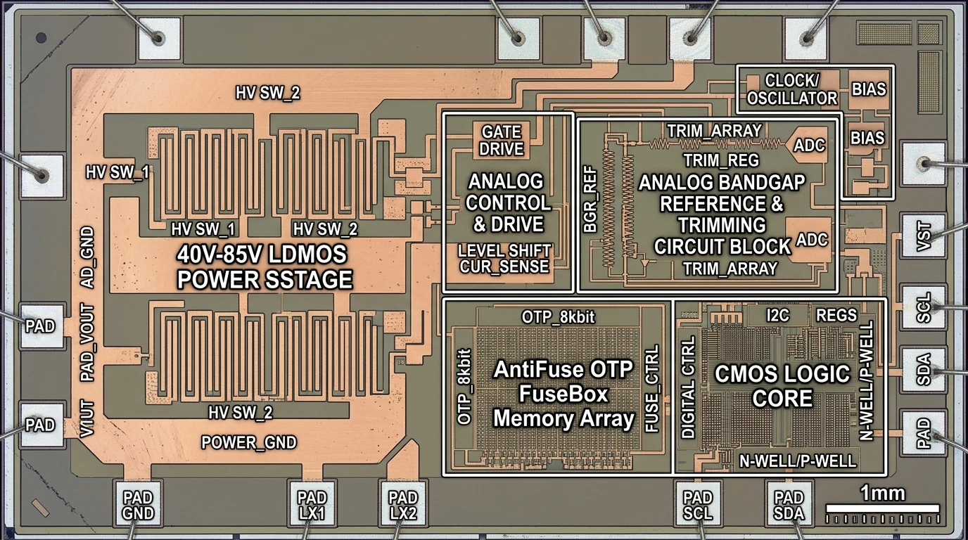
BCD 電源管理:從低密度精準修調到高密度通訊協議韌體 BCD Power Management: Bandgap Trimming, Motor Drivers & Protocol Chips
單晶片整合 Bipolar 精度、CMOS 邏輯與 DMOS 高壓耐受力。純邏輯 AntiFuse OTP 免除浮閘 eFlash 帶來的額外熱預算,確保 40V–85V LDMOS 崩潰電壓與車規高溫可靠性。 Monolithic integration of Bipolar precision, CMOS logic, and DMOS high-voltage capability. Pure-logic AntiFuse OTP eliminates eFlash thermal budget risks, preserving 40V–85V LDMOS breakdown voltages and automotive high-temp reliability.
1.1 低密度電性微調閉迴路(128-bit ~ 2K-bit) 1.1 Low-Density Trimming Closed-Loop Pipeline (128-bit to 2K-bit)
閉迴路校準 · 漂移消除CLOSED-LOOP CALIBRATION · DRIFT CANCELLATIONBCD 帶隙基準電壓 (Vref) 閉環修調時序與 AntiFuse 燒錄管線 BCD Bandgap Reference (Vref) Closed-Loop Trimming & AntiFuse Burn Pipeline
原生帶隙電壓採樣 Raw Bandgap Sense
SAR 最優微調碼合成 SAR Trim Code Synthesis
AntiFuse 物理細絲擊穿 AntiFuse Filament Rupture
電壓驗證與防篡改鎖定 Post-Trim Lock & Pass
1.2 高密度智慧協議與控制(高密度儲存,8KB ~ 64KB+/64Kb ~ 512Kb) 1.2 High-Density Smart Protocol & Control (8KB to 64KB+ / 64Kb to 512Kb)
韌體儲存 · MCU 整合FIRMWARE STORAGE · MCU INTEGRATION高密度智慧協議與控制:單晶片 32-bit MCU、eNVM 韌體與驅動級整合總線 Smart Protocol & Motor Control: 32-bit MCU, eNVM Firmware & Power Stage Bus
USB-PD 3.1 EPR 快充控制器 USB-PD 3.1 & EPR Controller
無刷馬達向量 FOC 控制器 Brushless Motor Vector FOC
車規電池管理與功能安全 Automotive Battery Safety
LFM 等度量須以具名 FMEDA 與 Tscrub 等 AoU 關閉,不得由本頁敘述直接推出。
SEooC AoU: ISO 26262 ASIL vocabulary only (not READY certification). IEC 61508 SC3 is a cross-standard teaching reference — this page does not claim that capability by architecture alone. Metrics such as LFM require named FMEDA and AoU bounds such as Tscrub — do not infer certification from this page.
BCD 製程專用 eNVM 代工生態:Tower Y-Flash、VIS/PSMC 億而得 (YMC) 與純邏輯 AntiFuse 縱深比較 Specialty BCD eNVM Foundry Matrix: Tower Y-Flash, VIS/PSMC YMC MTP & Logic AntiFuse Co-Optimization
在高壓 BCD(Bipolar-CMOS-DMOS)製程中,整合傳統雙層浮閘 eFlash 需面臨 8~12 道額外光罩與破壞功率元件耐壓的熱預算難題。業界主要 Specialty 代工廠與 IP 供應商發展出三條高度互補的 0-Mask 縱深路徑: Integrating conventional double-poly eFlash into high-voltage BCD (Bipolar-CMOS-DMOS) carries an 8-12 mask adder penalty and severe thermal budget impacts on power DMOS breakdown. Specialty foundries and IP providers have engineered three highly complementary zero-mask architectures:
BCD 帶隙電壓微調模擬與零光罩 (Zero-Mask) 經濟學試算器 BCD Bandgap Trimming Simulator & Zero-Mask Adder ROI Calculator
左側互動體驗 OTP 微調如何消除晶圓高斯常態分佈偏差;右側 ROI 使用固定假設光罩與晶圓差價(180nm:$650K/片 $80;55nm:$1.45M/片 $180)— 非報價或量測。 Left: interactive Vref trim demo. Right: ROI uses fixed assumed mask/wafer deltas (180nm: $650K / $80 per wafer; 55nm: $1.45M / $180) — not quotes or measured savings.
| 評估維度 (Metrics)Metrics & Criteria | AntiFuse OTP(固定)/NeoMTP(浮動閘 MTP)Antifuse OTP (Fixed) / NeoMTP (Floating-Gate MTP) | 傳統浮閘 eFlash (Floating-Gate)Legacy Floating-Gate eFlash | 工程決策影響Strategic Decision Impact |
|---|---|---|---|
| 額外光罩數Additional Mask Count | 0 道額外光罩0 Extra Masks (Zero Adder) | +10 至 +15 道光罩 (+30~50% 成本)+10 to +15 Masks (+30-50% Cost) | 縮短 Tape-out 時程與原型開模費用 (NRE)Compressing prototype turnaround and tapeout NRE costs |
| 高壓耐壓退化 (HV Impact)High-Voltage Degradation | 零額外熱衝擊Zero Impact (No extra thermal budget) | 製程約束 (高溫退火影響 LDMOS 漂移區耐壓)Process constraint (Thermal annealing affects LDMOS drift region) | 維持 40V–85V LDMOS 崩潰電壓與 SOA 安全工作區Preserves 40V–85V breakdown voltage and Safe Operating Area (SOA) |
| 車規高溫資料保存 (Retention)High-Temp Retention | 15+ 年 @ 175°C Tj(原列選型目標,依 IP 分別驗證);AntiFuse:擊穿路徑;NeoMTP:浮動閘電荷15+ yrs @ 175°C Tj (listed selection target; validate each IP); Antifuse: breakdown path; NeoMTP: floating-gate charge | >125°C 漏電加劇 (SILC 氧化層洩漏)Degrades >125°C due to SILC oxide leakage | 滿足車用動力系統與底盤 AEC-Q100 Grade 0 要求Crucial for AEC-Q100 Grade 0 automotive powertrain and chassis |
| 超低功耗待機(待機漏電)Standby Power & Leakage | < 1 pA (無接面逆向漏電)< 1 pA Zero-Junction Standby Leakage | BCD 接面漏電較高 (消耗待機電流)Higher BCD junction leakage consumes standby current | 賦予電子貨架標籤 (ESL) 與物聯網節點 5–10 年電池壽命Enables 5–10 year coin-cell battery lifetime for ESL and IoT nodes |
第三代半導體 SiC/GaN 閘極驅動晶片:奈秒死區微調、去飽和保護與抗 CMTI 高溫實踐 SiC/GaN Gate Drivers: Nanosecond Dead-Time Trimming, DESAT Protection & High-CMTI Resilience
在 800V 電動車主驅逆變器與 AI 伺服器高密度電源中,碳化矽 (SiC) 與氮化鎵 (GaN) 以 >500kHz 高頻開關運行。封裝極小(SOIC-8/16)的高低側隔離閘極驅動晶片(如 TI UCC217xx、Infineon EiceDRIVER™、STGAP 系列)無法容納外掛 Flash,且須在 >150 V/ns 的極端共模瞬態 (CMTI) 與 175°C 結溫下保證零失誤: In 800V EV traction inverters and AI server power units, SiC and GaN switch at >500kHz. Highly constrained isolated gate driver ICs (TI UCC217xx, Infineon EiceDRIVER™, STGAP) cannot fit external Flash and must endure >150 V/ns CMTI transients at 175°C Tj:
奈秒級死區微調:在晶圓與成測時透過片上 AntiFuse OTP 燒錄 0.5ns 步進校準碼,壓縮傳遞延遲漂移,杜絕上下橋臂直通 (Short-Through)。 Sub-nanosecond Dead-Time Trim: Calibrated via on-chip AntiFuse OTP in 0.5ns steps to eliminate propagation skew and prevent bridge cross-conduction.
去飽和短路保護閾值:精確微調 6V–9V 故障偵測門檻與軟關斷 (Soft Turn-Off) 電流斜率,在 2µs 內安全關斷以拯救昂貴的 SiC 功率模組。 DESAT Fault Threshold: Trims 6V–9V trip voltages and soft turn-off slew rates, securing <2µs shutdown to save expensive SiC modules.
極端抗擾與高溫留存:AntiFuse 歐姆矽微絲具備天然抗位移電流雜訊能力;高壓 BCD Cascode 隔離免除浮閘氧化層高場擊穿老化風險。 CMTI Immunity & Retention: Ohmic filaments inherently resist displacement noise; cascode isolation protects against high-field dielectric wear.
高密集度矩陣修復:CIS 感光元件與 DRAM / HBM 晶圓良率守護 Dense Matrix Array Defect Repair: CIS Image Sensors & DRAM/HBM Yield Recovery
當像素陣列或記憶體單元格密度達到數千萬至數十億時,單一微塵或晶格位錯足以導致晶粒報廢。透過內建備援單元(Spare Rows / Columns)並配合 AntiFuse OTP 進行非揮發性硬體重映射,成為挽救數千億美元半導體產能的必備防線。 When pixel arrays or memory cells scale into millions and billions, a single defect causes fatal die loss. Deploying redundant spare elements and remapping defective addresses via AntiFuse OTP secures multi-billion-dollar semiconductor yields.
2.1 密集陣列自主缺陷掃描與 AntiFuse 重映射管線 2.1 Dense Array Defect Scan & AntiFuse Remap Pipeline
BIST / BIRA · 硬體修復BIST / BIRA · HARD REMAP自主缺陷檢測、備援覆蓋求解與 AntiFuse 物理重映射流程 Autonomous Defect Scan, Redundancy Solver & AntiFuse Hard Remap
BIST 陣列自檢雷達 BIST Radar Scan Engine
BIRA 備援啟發式解算 Heuristic Greedy BIRA Solver
AntiFuse 物理重映射 AntiFuse Hard Remap
自主矩陣缺陷修復掃描器 Autonomous Matrix Defect Repair Simulator (BIST / BIRA / AntiFuse)
點擊下方按鈕,體驗高密度矽晶矩陣在檢測到微塵物理缺陷後,如何藉由 BIST 掃描、BIRA 解算並以反熔絲暫存器重新映射,將良率從 0% 瞬間復原至 100%。 Click controls below to simulate real-time defect detection, March C- BIST scanning, BIRA spare row/column allocation, and AntiFuse OTP burning to restore die yield from 0% to 100%.
高密集陣列應用:3D 堆疊 CIS 壞點微調與 DRAM / HBM3e JEDEC hPPR 現場救援 Dense Matrix Applications: 3D-Stacked CIS Pixel Repair & HBM3e JEDEC hPPR
CMOS 影像感測器 (CIS) 壞點修復 CMOS Image Sensor (CIS) Pixel Repair
DRAM / HBM3e 封裝後現場修復 (PPR) DRAM / HBM3e Post-Package Repair (PPR)
修復熔絲技術代際演進:雷射熔斷 ➔ 電致遷移 ➔ 反熔絲微觀擊穿細絲 Fuse Technology Evolution: Laser Fuse ➔ eFuse ➔ AntiFuse Oxide Breakdown Nanofilament
雷射開窗物理熔斷 (Laser Fuse) Laser Ablation Fuse
碎屑與濕氣風險DEBRIS & MOISTURE RISK
電致遷移電熔絲 (Poly eFuse) Electromigration eFuse
熱再生長風險THERMAL GROW-BACK RISK
反熔絲閘極介電質擊穿細絲 (AntiFuse OTP) AntiFuse Dielectric Rupture Filament
永久擊穿導電通路PERMANENT BREAKDOWN PLUG
3D 堆疊 CIS 像素修補與 HBM3/DDR5 JEDEC PPR 硬體重映射實踐 3D-Stacked CIS Defect Repair & HBM3/DDR5 JEDEC PPR Silicon Implementation
Sony / OmniVision 3D 背照式 CIS 像素修補 Sony / OmniVision 3D BSI CIS Pixel Repair
Cu-Cu DBI 鍵合Cu-Cu DBI Bonded感光像素晶粒與邏輯晶粒透過 Cu-Cu 混合鍵合 (DBI) 堆疊。晶圓測試 (CP) 時檢測出成千上萬個暗電流亮點 (Hot Pixels)。嚴禁採用傳統 eFlash:因 >900°C 退火會熔毀已塗佈之彩色濾光片與微透鏡;嚴禁雷射熔斷:因封裝後雷射無法穿透矽層。常見架構為 0-Mask 純邏輯 AntiFuse OTP,在室溫探針測試下以電氣脈衝硬鎖定數十 Kb 壞點座標 — 具名產品仍須對照 PDK 與修復流程,非全族唯一解。 Pixel dies bond to logic dies via Cu-Cu DBI. Testing flags thousands of hot pixels. eFlash is forbidden as >900°C anneal destroys color filters and microlenses; laser fuses are inaccessible inside stacked 3D dies. A common architecture is zero-mask logic AntiFuse OTP that electrically locks defect coordinates at room temperature — named products still need PDK/repair-flow evidence; not a universal-only solution.
JEDEC DDR5 / HBM3 Hard-PPR 封裝後修復 JEDEC DDR5 / HBM3 Hard-PPR Post-Package Repair
JESD79-5 / JESD238JEDEC 標準定義了封裝後硬體重映射 (Hard Post-Package Repair, hPPR)。傳統 Poly eFuse 因電致遷移空隙具備熱鬆弛回跳 (Grow-Back) 致命缺陷,在伺服器高溫環境下易使已修復壞位元死灰復燃;而 AntiFuse 的局域再結晶矽微絲為永久性歐姆通道 (R < 100Ω),在 150°C~175°C 高溫下具備零回跳與永久性物理鎖定,成為高頻寬記憶體 (HBM3/HBM3e) 與 DDR5 模組良率的產業黃金基準。 JEDEC defines Hard Post-Package Repair (hPPR). Conventional poly eFuses suffer thermal grow-back, risking defect reappearance under server heat. AntiFuse forms permanent recrystallized ohmic silicon filaments (R < 100Ω) with zero grow-back across 150°C~175°C, serving as the gold standard for DDR5 and HBM3 stack yields.
高壓顯示驅動 (HV DDIC):Gamma 校準、Vcom 防閃爍與 De-Mura 補償 High-Voltage Display Drivers: Gamma Tuning, Vcom Anti-Flicker & De-Mura
顯示面板驅動 IC(DDIC)整合了雙重耐壓域:高壓端 Gate Driver 承受高達 35Vp-p 峰對峰擺幅(V_GH = +20V, V_GL = -15V,製程耐壓安全裕度達 40V),類比端 Source Driver 則為高速高精度 8V ~ 12V(AMOLED 子像素驅動可達 16V)。內嵌 eNVM 必須在嚴苛的高壓環境中長期抵抗電氣干擾,精準儲存光學校準參數與灰階查找表。 Display Driver ICs (DDICs) partition into dual voltage domains: Gate Drivers handle 35Vp-p swings (V_GH = +20V, V_GL = -15V with 40V process breakdown margin), while Source Drivers operate at 8V~12V (up to 16V for AMOLED sub-pixels). Embedded eNVM must withstand high-voltage electrical stress to preserve optical calibration registers and color correction tables.
3.1 高壓顯示光學補償與 Gamma 校準管線 3.1 High-Voltage Display Optical Compensation & Gamma Pipeline
光學訊號鏈 · 閉環微調OPTICAL SIGNAL CHAIN · CLOSED-LOOP TRIM高壓顯示面板光學訊號鏈:Vcom 防閃爍 ➔ Gamma 2.2 R-DAC ➔ OLED De-Mura 補償 Display Optical Signal Chain: Vcom Centering ➔ Gamma 2.2 R-DAC ➔ 2D De-Mura Compensation
Vcom 共同電極中心微調 Vcom Center Calibration
Gamma 2.2 階梯 R-DAC 映射 Gamma 2.2 R-DAC Curve
OLED 2D De-Mura 空間補償 2D OLED De-Mura Compensation
高壓顯示光學調節器 (Gamma 2.2、Vcom 頻閃消除與 De-Mura 補償) High-Voltage Display Optical Tuner (Gamma 2.2, Vcom Anti-Flicker & De-Mura)
左側滑動調節 Gamma 曲線與觀察色階輸出;右側 De-Mura 均勻度/ΔE 為固定假設示意(74.2%→99.4%、3.8→0.45),非光學量測。 Left: Gamma curve tuner. Right: De-Mura uniformity/ΔE uses fixed teaching assumptions (74.2%→99.4%, 3.8→0.45) — not optical measurement.
高壓與特種製程 Hard IP:從測試晶片流片到車規可靠度封閉全流程 High-Voltage Hard IP Rigor: From Test Chip Tapeout to Reliability checklist
NVM 是極度敏感的實體 Hard IP,絕非可任意合成轉移的軟體 RTL。代工廠具備特定高壓或特種製程,絕不代表矽智財廠商已有現成 Macro 布局。每一個特定金屬層堆疊(Metal Stack)與 PDK 變體,均必須歷經獨立的專屬測試晶片(Test Chip)流片、全溫區 PVT Corner 特性化實測與車規級加速老化驗證。 Embedded NVM is custom physical Hard IP, not portable generic RTL. A foundry offering a specialty process does NOT imply Silicon IP availability. Every specific metal stack and PDK variant mandates dedicated test chip tapeouts, multi-lot PVT corner characterization, and automotive reliability checklist.
特種高壓製程實體 IP 晶圓驗證三道簽核流程 Specialty HV Hard IP Silicon verification checklist pipeline
NVM 為客製實體 Hard IP,非軟體 RTL。每一 PDK 變體必須嚴格通過三道實體晶圓門禁簽核: Embedded NVM is custom physical Hard IP. Every PDK variant mandates 3 silicon verification checklist gates:
3-Lot 晶圓流片與 Shmoo 裕度3-Lot Tapeout & Shmoo Matrix
- 晶圓批次:Wafer Lots: 專屬測試晶片跨 3 批次 (3-Lot)Dedicated 3-Lot test vehicles
- 溫度跨度:Temp Range: -40°C ~ 150°C / 175°C
- 電壓裕度:Voltage: ±10% VDD Core / IO Shmoo
- 物理指標:Physical: 細絲電阻 <100Ω 4σ 分佈Filament R < 100Ω 4σ fit
高壓脈衝隔離與 HTOL 老化HV Noise Isolation & HTOL Qual
- 隔離架構:Isolation: Deep N-Well 三重基板保護環Deep N-Well guard-rings
- 耐受指標:dV/dt: 50V/ns 高速瞬態脈衝抑制50V/ns pulse suppression
- 加速老化:Stress: 1000 小時 HTOL + HTSL 烘烤1000h HTOL + HTSL bake
- 電荷保存:Retention: 消除浮閘 SILC 電荷流失路徑;關斷漏電 <0.1 pA/cell,15+ 年 @ 175°C TjEliminates floating-gate SILC loss path; standby leakage <0.1 pA/cell, 15+ yrs @ 175°C Tj
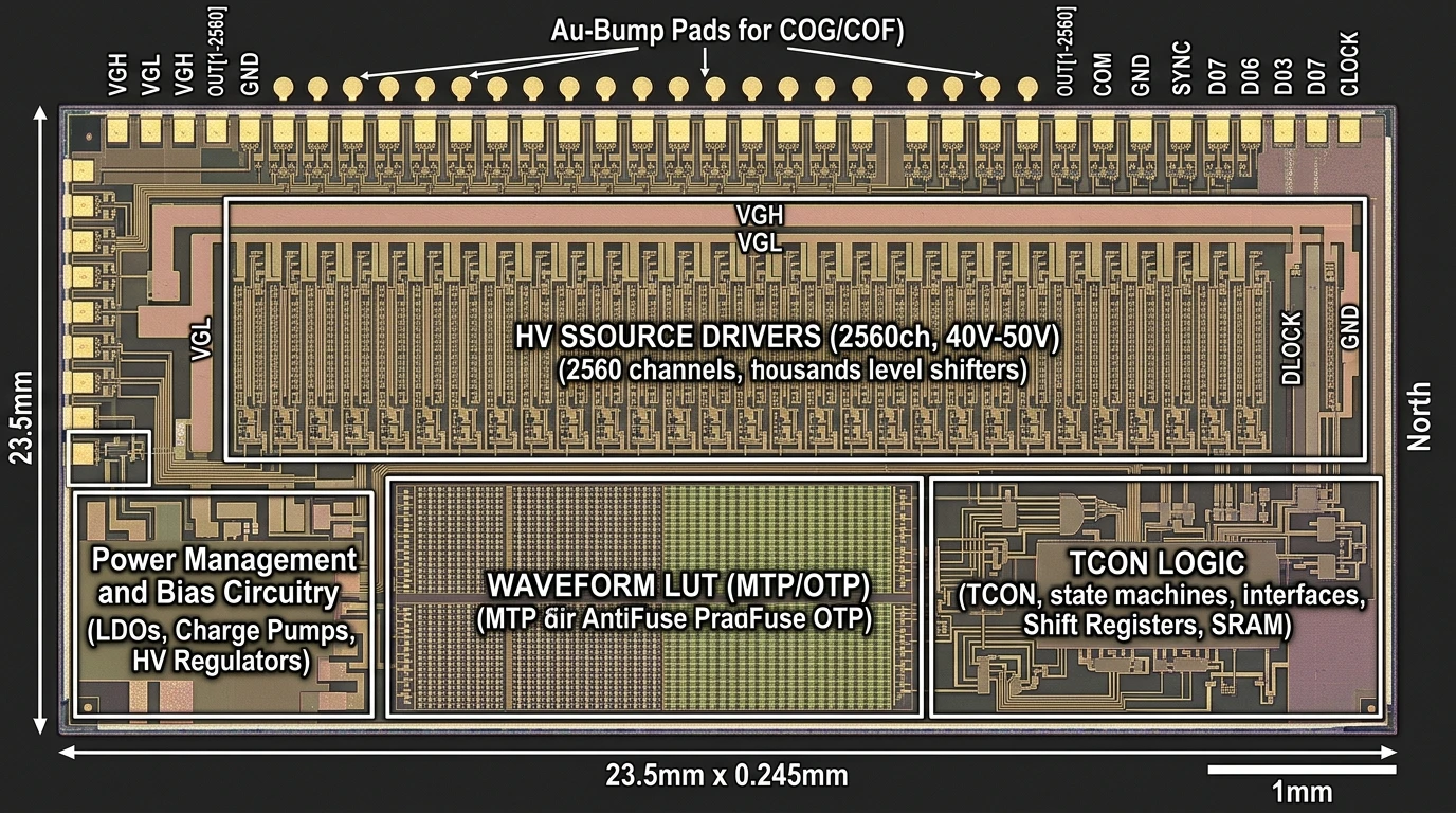
COG/COF 金凸塊與 260°C 迴焊COG/COF Au-Bumps & Reflow
- 幾何極限:Form Factor: Macro 高度嚴格限制 <250μmMacro height < 250μm
- 晶圓薄化:Thinning: 打薄至 <100μm 應力無裂紋Thinning <100μm zero crack
- 接合剪切:Shear: Au-bump 剪切力 >15g/mil²Au-bump shear > 15g/mil²
- 熱應力:Reflow: J-STD-020 260°C 無鉛迴焊通過J-STD-020 260°C reflow pass
OLED 顯示驅動 (DDIC) 逐點 De-Mura 光學補償與超低引腳數外掛 NOR 封裝革新 AMOLED DDIC Point-by-Point De-Mura & Ultra-Low Pin Count Serial NOR Innovation
Novatek / Himax AMOLED De-Mura 數據暴增挑戰 Novatek / Himax AMOLED De-Mura Data Scaling Challenge
FHD+/WQHD+ 二維網格FHD+ / WQHD+ 2D Grid高階 AMOLED 面板由於有機發光材料沉積的不均勻性,需外置相機高精掃描並生成 2D 亮度/色度差分補償矩陣 (De-Mura)。隨面板解析度自 FHD+ 提升至 WQHD+,De-Mura 數據量自數十 KB 暴增至 4MB~16MB。若將其全部內嵌於高壓製程 (28nm/40nm HV) 晶粒內,高壓 eFlash 面積開銷過巨,將嚴重損害 DDIC 長條形晶粒 (Aspect Ratio > 20:1) 的良率與晶圓產出。 AMOLED panels exhibit pixel luminance variations requiring factory optical scanning to generate 2D De-Mura matrices. As resolutions reach WQHD+, De-Mura data explodes from tens of KB to 4MB~16MB. Monolithically embedding this into 28nm/40nm HV DDIC dies inflates silicon area, devastating yields for ultra-narrow aspect ratio (>20:1) dies.
內部 0-Mask OTP + 外部/合封 Ultra-Low-Pin NOR 雙軌解法 Internal 0-Mask OTP + External Ultra-Low-Pin NOR Hybrid Route
WLCSP / USON / Octal SPI產業主流轉向分層儲存:核心電氣參數 (Vcom、Gamma 曲線、晶片安全 ID) 採用晶片內 0-Mask 純邏輯 AntiFuse OTP / MTP 永久硬鎖定,抵抗高壓電氣雜訊;龐大之 De-Mura 點矩陣 則透過高速 Octal SPI / xSPI 介面串接外掛或 COF (Chip-on-Film) 上合封之 Winbond / Macronix 1.2V 超低引腳數 Serial NOR Flash (WLCSP 或超薄 USON 封裝),於開機時極速 DMA 載入內部 SRAM,兼顧極致窄邊框與最低系統 BOM 成本。 Industry adopts a tiered hybrid: Critical electrical parameters (Vcom, Gamma, security ID) are locked on-chip via 0-mask logic AntiFuse OTP/MTP against HV noise; massive 2D De-Mura matrices stream via high-speed Octal SPI from co-packaged Winbond/Macronix 1.2V ultra-low-pin Serial NOR Flash (WLCSP/USON on COF), balancing razor-thin display borders with optimal BOM.
電子紙 (E-Ink) 超高壓驅動:40V-50V 脈衝波形與 MTP ➔ OTP 演進 E-Ink Ultra-HV Driving: 40V-50V Waveforms & MTP-to-OTP Migration
雙穩態電泳顯示(EPD)憑藉超低功耗與陽光下高可讀性,已橫掃電子貨架標籤(ESL)與電子閱讀器市場。然而,驅動微膠囊中帶電色素微粒子需要高達 40V 至 50V 的超高壓雙極性脈衝。 Bistable electrophoretic displays (EPD) dominate Electronic Shelf Labels (ESL) and e-readers through near-zero static power. However, moving charged pigment particles inside microcapsules demands 40V to 50V ultra-high-voltage bipolar pulses.
4.1 超高壓電泳波形時序與雙穩態狀態機 4.1 Ultra-HV Electrophoretic Timing & Bistable State Machine
40V-50V 波形 · 雙穩態驅動40V-50V WAVEFORM · BISTABLE DRIVER40V-50V 雙極性電泳驅動波形時序與 MTP ➔ OTP 產品生命週期狀態機 40V-50V Bipolar Electrophoretic Waveform Timing & MTP-to-OTP State Machine
微粒活化與殘影擦除 (Shake & Reset) Agitation & Erase Pulse
克服黏滯阻力OVERCOMES VISCOUS DRAG
目標推升與雙穩態休眠 (Drive & Rest) Target Drive & Bistable Rest
零靜態功耗ZERO STATIC POWER DRAIN
eNVM 產品生命週期演進 MTP to OTP Migration
晶圓成本降低 35%35% WAFER COST REDUCTION
電子紙微膠囊電泳物理與高壓波形示波器 E-Ink Electrophoretic Physics & High-Voltage Waveform Oscilloscope
切換不同顯示模式,觀察微膠囊中帶電色素微粒子的受力沉浮過程、實時示波器 40V-50V 驅動脈衝序列,以及對應的 MTP ➔ OTP 演進決策。 Switch display modes to witness charged pigment microparticle migration under 40V-50V pulses, real-time waveform oscillograms, and MTP-to-OTP architecture migration indicators.
彩色粒子配方與微膠囊製程快速疊代演進中。採用 32 K-bit ~ 64 K-bit (4 KB ~ 8 KB) MTP 保持在線波形查表 (LUT) 更新彈性。 Color particle formulation is evolving. Deploying 32 K-bit to 64 K-bit (4 KB to 8 KB) MTP ensures flexibility for in-field waveform LUT updates.
| 比較維度 (Factor / Feature)Factor / Feature | 電子紙 (E-Ink / EPD)E-Ink / EPD | 液晶與有機發光 (LCD / OLED)LCD / OLED | 驅動晶片與 eNVM 關鍵意涵DDIC & eNVM Strategic Impact |
|---|---|---|---|
| 畫面動態更新Motion Display | 偏慢 (數百毫秒粒子電泳)Slow (Hundreds of ms particle migration) | 即時 (60Hz - 144Hz 更新率)Real-time (60Hz - 144Hz refresh rate) | 電子紙需要依據溫度調用多幀波形序列 (Waveform Frames)E-Ink requires temperature-dependent multi-frame waveform lookups |
| 能源消耗特性Energy Consumption | 雙穩態 (僅在畫面更新時耗電)Bistable (Power only at content change) | 持續耗電 (需背光或持續驅動電流)Constant power draw (Continuous backlight/current) | 極低待機漏電;以內嵌 eNVM 取代離散 Flash 降低系統待機功耗Low standby leakage; embedded eNVM replaces external Flash to reduce standby draw |
| 驅動電壓水準Drive Voltage Rails | 40V 至 50V 雙極性電泳脈衝40V to 50V Bipolar Electrophoretic Pulse | Gate 35Vp-p (+20V/-15V) / Source 8V-16V (40V 製程裕度)Gate 35Vp-p (+20V/-15V) / Source 8V-16V (40V Process Margin) | 受限 COG/COF 極致長寬比 (<250µm) 與多通道高密度,BCD 製程在尺寸與金屬層數上受限,採用專屬 110HV / 90HV 高壓 CMOSDue to ultra-slim die aspect ratio (<250µm for COG/COF) and high channel density, BCD is constrained by layout; mandates dedicated 110HV/90HV High-Voltage CMOS |
| 全彩顯示能力Full Color Capability | 演進中 (黑白 ➔ 4 色 ➔ Spectra 6 / Kaleido 3)Evolving (Mono ➔ 4-Color ➔ Spectra 6 / Kaleido 3) | 純熟原生全彩 (RGB 16.7M 色以上)Mature native full color (16.7M+ colors) | 演進期以 32 K-bit ~ 64 K-bit (4 KB ~ 8 KB) MTP 保持波形更動彈性,成熟後轉入低成本 OTP32-64 K-bit (4-8 KB) MTP ensures code flexibility during color evolution; OTP for mature high volume |
| 環境強光可讀性Sunlight Readability | 優良環境光對比 (反射式架構,陽光下保持可讀)High ambient contrast (Reflective; readable under direct sunlight) | 對比度受限 (需提高背光亮度對抗強光反射)Contrast reduced (Requires increased backlight brightness to overcome ambient light) | 大型戶外公車站看板需串聯更多顆 Driver ICLarge outdoor signage cascades numerous driver ICs, multiplying NVM TAM |
| 核心應用場景Key Applications | ESL 電子貨架標籤、電子書、戶外全彩廣告牌、車身/建築裝飾 (Prism 3)ESL electronic shelf labels, e-readers, outdoor color billboards, Prism 3 automotive skins | 智慧手機、筆電、電視、車用儀表座艙Smartphones, laptops, TVs, automotive digital cockpits | 電子紙市場年複合成長率 (CAGR) 顯著,帶動特種 eHV eNVM 需求擴展E-paper market CAGR expands specialty eHV eNVM demand across retail and outdoor infrastructure |